8085 Circuit Diagram
Microprocessor based home security system – electronics project Intel microprocessor basic addressing diagram modes 8085 microprocessor addressing
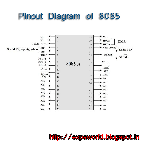
WORLD OF EMBEDDED: Pin-out diagram of 8085
Interfacing 8085 rom microprocessor Basic microprocessor's (intel 4004 and 8085). « sadaf media 8085 microprocessor pin diagram explained
8085 microprocessor: architecture, pin diagram
8085 motor dc microprocessor based control speed system using controller datas electrical scienceI need a wiring/circuit schematic of a specific 8085 starter kit What is the difference between 8085 and 8086 microprocessor8085 diagram microprocessor description pdf circuit various code microprocessors board address electronics chip general purpose bit choose mpu.
Tech-experts: intel 8085 block diagram8085 microprocessor study notes for electronics and communication 8085 microprocessor registersInside the alu of the 8085 microprocessor.

Intel 8085 microprocessor architecture and programm..
8085 diagram embeddedMicroprocessor system based security project diagram circuit 8085 circuits systems hardware board electronics divided alarm projects control parts telephone also External memory interfacing in 8085: ram and rom8085 microprocessor architecture ic.
8085 architecture : pin diagram and its addressing modesWorld of embedded: interfacing of 8255 with 8085 processor 8085 pin diagram pinout connection diagram8085 diagram microprocessor configuration description pinout integrated elektropage electronics those circuits electronic introduction teacher ic technology engineer.

8085 microprocessor architecture internal intel diagram block bus microprocessors programming bcis notes appropriate
8255 8085 interfacing processor embeddedA "media to get" all datas in electrical science...!!: 8085 Blog archivesWorld of embedded: pin-out diagram of 8085.
8085 architecture microprocessor alu arithmetic geeksforgeeks unit logic8085 pin diagram 8085 architecture : pin diagram and its addressing modesMicroprocessor diagram architecture depicts following.

Alu microprocessor negation
8085 microprocessor architecture diagram timing electronics control address data circuitry club instruction registers logic buffer unit machine click cycle differentArchitecture of 8085 microprocessor Stepper interface interfacingEducation for all: functional block diagram of 8085 microprocessor.
8085 microprocessor ic8085 diagram block intel processor presentation ppt powerpoint its instruction set 8085 microprocessors functional signals8085 diagram block intel tech registers data register these experts bit hold.

8085 microprocessor architecture difference intel between unit control register pediaa features important
Introduction to microprocessor 8085 and pin diagram part1 ~ engineeringMicroprocessor diagram signals engineering notes 8085 registers microprocessor directly refereeing respective programmerMicroprocessor architecture 8085 diagram block functional function diagrams microprocessors 8086 logic structure alu computer book bus microcontrollers education buses electronics.
8085 pin diagram8085 diagram microprocessor description explanation signals pdf bus explained 8085 programming: 8085 pin out diagram.

8085 Architecture | Intel 8085 Processor Architecture Block Diagram

8085 Microprocessor Study notes for Electronics and Communication

8085 Pin Diagram | Microprocessors Tutorials | Teachics
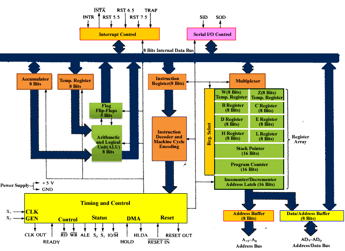
Tech-Experts: Intel 8085 Block Diagram

8085 Microprocessor: Architecture, Pin Diagram - Electronics Club

8085 Architecture : Pin Diagram and Its Addressing Modes

External memory interfacing in 8085: RAM and ROM